FRAM Write Block Description
This block enables writing data to a non-volatile Ferroelectric Random Access Memory (FRAM) chip via a Serial Peripheral Interface (SPI).
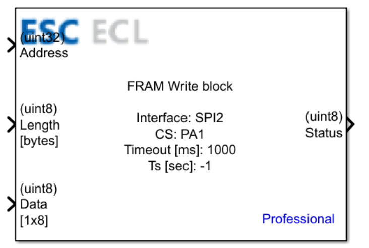
Table of Contents
Inputs
| Input Name | Type | Description |
|---|---|---|
| Address | uint32 | The target base memory address within FRAM memory where data will be stored. |
| Length [bytes] | uint8 | The total number of consecutive bytes from the input array that will be written to the memory chip. |
| Data | uint8[1x8] | An array containing the raw payload bytes intended to be written to the external FRAM memory chip. |
Outputs
| Output Name | Type | Description |
|---|---|---|
| Status | uint8 | Outlines the operational execution status of the SPI communication routine:1 – write operation completed successfully0 – communication failure or transaction timeout |
Block Parameters
| Parameter | Description |
|---|---|
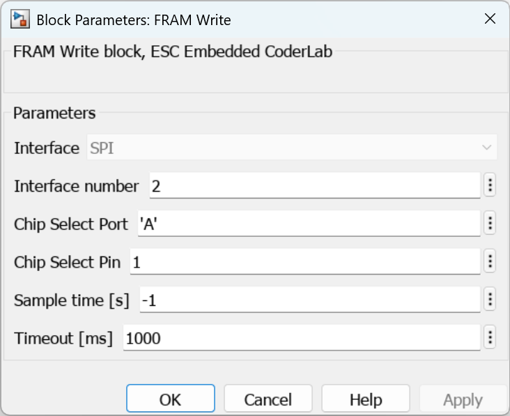
| Interface | Selection of the communication interface standard (default fixed to SPI). |
| Interface number | Specifies the hardware instance identifier index of the SPI peripheral embedded on the MCU. |
| Chip Select Port | The GPIO port group letter designated for the active-low slave select signal (Chip Select). |
| Chip Select Pin | The physical hardware pin number belonging to the chosen Chip Select Port. |
| Sample time [s] | Specifies the software cyclic refresh execution update interval for the block. |
| Timeout [ms] | The maximum duration in milliseconds allowed for the hardware SPI driver transaction query to complete before throwing an error. |
CubeMX Configuration for a Given MCU Model
To configure CubeMX for a given microcontroller model, you must set up the SPI interface according to the provided instructions.
See Also
Last updated on